The global Chip shortage that began in the autumn of 2020 will last for a whole year in 2021, but this trend has not eased. The semiconductor industry is expanding production capacity and actively upgrading processes to improve productivity. On the other hand, COVID-19 continues to mutate, and the continuation of the epidemic continues to have an impact on the entire semiconductor industry. The formation of telecommuting, online meeting and online education habits has accelerated the Digital transformation of several industries, and has also promoted the technological upgrading of network communication, artificial intelligence, storage and cloud services from the side.
Batch production using 13nm technology
In terms of cutting-edge semiconductor manufacturing processes, Samsung OEM temporarily adjusted 4LPE to a complete process node in 2020. That is to say, the 4nm process will become the focus of Samsung's promotion in the next period of time. In October 2021, TSMC announced that there was a slight delay in the N3 process, and 2022 may become the year of the 4nm process. There is almost no hope that iPhone 14 will catch up with the 3nm process.
But basically, it is clear that although the fastest chip to use TSMC's N3 process may need to wait until the first quarter of 2023, mass production of the N3 process is clearly expected until the fourth quarter of 2022.
We believe that Samsung 3nm GAA may be a bit later than TSMC N3. Samsung began using GAA structured transistors as a focus at 3nm nodes, but in fact, Samsung also failed to advance as scheduled. Moreover, according to Samsung's current publicly available data, its earliest 3nm process may face greater technical uncertainty.
As for Intel 3, it is completely unable to catch the 2022 bus. TSMC N3 will continue to maintain its dominant market position, temporarily leading the other two competitors. But stepping on the brake of N3 actually laid a hidden danger for the arrival of the 2nm era.
On the one hand, the Intel 20A process is expected to be launched in the first half of 2024. Intel 18A may appear in the second half of 2025- Intel's determination to return to technology leadership at these two nodes is quite firm. On the other hand, Samsung is expected to mass produce the 2nm process in the second half of 2025. This will be its third generation GAA structure transistor, meaning that although its 3nm process may not gain market dominance, this technology will provide strong support for its 2nm process. These all increase the uncertainty of the subsequent 2nm process market competition.
2 DDR5 standard memory entering mass production and commercial use
On July 15, 2020, in order to address the performance and power consumption challenges faced by a wide range of applications, from client systems to high-performance servers, the Solid State Technology Council (JEDEC) officially released the final specification of the next-generation mainstream memory standard DDR5 SDRAM (JESD79-5), ushering in a new era of global computing memory technology. JEDEC describes DDR5 as a "revolutionary" memory architecture and believes that its emergence marks the industry's transition to DDR5 server dual in-line Memory module (DIMMs)

DDR5 type
According to data from market research firm Omdia, the market demand for DDR5 has been increasing since 2020. By 2022, DDR5 will account for 10% of the entire DRAM market and expand to 43% by 2024. In 2023, DDR5 will be widely adopted in mainstream markets such as mobile phones, laptops, and personal computers, with shipments significantly exceeding DDR4, completing a rapid transition between the two technologies.
The growth rate of Memory bandwidth is far faster than the processor performance, which is the basic driving force for the introduction of DDR5. However, unlike previous product iterations, this product mainly focuses on reducing power consumption and prioritizing PC as an application. The industry generally believes that DDR5 will emulate DDR4 and occupy a leading position in the data center.
The most eye-catching aspect of DDR5 is that it is faster than the already "super fast" DDR4. Compared to the maximum 3.2Gbps transmission speed of DDR4 memory at a 1.6GHz clock frequency, the new DDR5 memory achieves a maximum transmission speed of 6.4Gbps and synchronizes the power supply voltage from 1.2V to 1.1V of DDR4, further improving the energy efficiency performance of the memory.
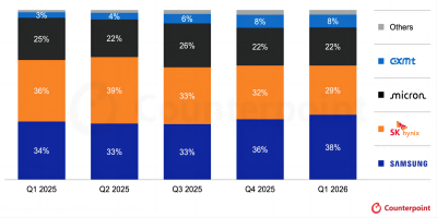
At present, Samsung, SK Hynix, Micron and other global storage giants have announced the mass production and commercial schedules of their DDR5 products. However, DDR5 will not be launched overnight and requires strong support from the ecosystem, including system and chip service providers, channel providers, cloud service providers, and original equipment manufacturers.
3 DPU market cake continues to grow and explode
The nickname of the Democratic Party became popular at the end of 2020. We believe that the market behavior that made the term DPU popular is: firstly, NVIDIA acquired the Israeli company Mellanox, which created the term "DPU" the following year; Secondly, the startup company Fungible vigorously promoted the name DPU in the same year.
The D in DPU represents DATA data. Smart network cards have rapidly developed into DPU data processors. With lightning speed, dozens of DPU startups have emerged in a short period of time.
DPU is essentially the evolution of smart network cards, but it is not difficult to see from the enthusiasm of DPU that data centers have a strong desire for dedicated processors in the data direction and further formalization and standardization.

Data processing unit
In the early days of data centers, there was a term called "data center tax", meaning that servers purchased many core CPUs. But for the final business, some of these cores are "nibbled" by default. Because these processor resources need to be used for data virtual networking, security, storage, virtualization, and other tasks. As these tasks become increasingly complex, DPU appears. Just as graphical computing has GPUs and artificial intelligence computing has NPUs, DPUs are a product of the rise of specialized computing in this era.
Generally speaking, the work of a DPU includes: first, uninstalling the original CPU OVS, storage, security services, and other activities; Secondly, the management system management program should be isolated and virtualized; Thirdly, further accelerate cross node data processing through various means.
It is not difficult to understand that DPU has become the standard for data centers. However, in terms of specific implementation, different DPUs should not be on the same stage, as they play different roles. For example, although Intel's IPU is also a DPU, it still differs from NVIDIA DPU in terms of responsibility and work bias. Therefore, the DPU market may be segmented. And data center systems companies are researching their own more adaptable DPUs, which brings uncertainty to the DPU market.
4 Storage and computing integration across "storage walls" and "power walls"
The formation of the concept of processing in memory (PIM) can be traced back to the 1970s, but this concept is limited due to the complexity of chip design and manufacturing costs and the lack of killer Big data applications to drive it.
In recent years, with the progress of chip manufacturing technology and the development of artificial intelligence applications, the functions of processors have become increasingly powerful, with faster speeds and larger storage capacity. In the face of massive data, slow data processing speed and high processing energy consumption have become computational bottlenecks. When extracting data from memory outside the processing unit, the processing time is often hundreds or thousands of times longer than the calculation time, and the energy consumption of the entire process is roughly between 60% and 90%, resulting in very low efficiency.
On the other hand, Moore's law, which is close to the limit, and the Von Neumann architecture limited by the storage wall can no longer meet the needs of this era in terms of computing power enhancement. The current non von Neumann architecture that attempts to solve the problems of "storage walls" and "power walls" includes low-voltage subthreshold digital logic ASICs, neural morphology, and analog computing. The non von Neumann architecture includes low-voltage subthreshold digital logic ASIC, neural morphology computing, and analog computing, among which memory computing integration is the most direct and effective.
This is a new computing architecture that can perform two-dimensional and three-dimensional Matrix multiplication operations instead of optimizing on traditional logical computing units. This can theoretically eliminate the delay and power consumption of data transmission, improve the efficiency of artificial intelligence computing by hundreds of times and reduce costs, making it particularly suitable for neural networks.
5 5G construction focuses on autonomous networking and millimeter wave
With fiber optic speed, ultra-low latency, and network capacity, 5G has the same impact as electricity, completely changing all industries.
As a powerful complement to the Sub-6GHz band, the 5G millimeter wave has outstanding advantages such as high frequency broadband capacity, easy integration with beam fugacity, and ultra-low delay, which is conducive to promoting the development of industrial Internet, AR/VR, cloud games, Real-time computing and other industries. At the same time, millimeter waves can support high-precision positioning and dense area deployment with high equipment integration, which will help promote the miniaturization of base stations and terminals.
According to GSMA's "Millimeter Wave Application Value" report, by 2035, 5G millimeter waves are expected to generate $565 billion in global GDP and generate $152 billion in taxes, accounting for 25% of the total value created by 5G.
At present, 186 operators from 48 countries are planning to develop 5G in the millimeter wave spectrum of 26-28 GHz, 37-40 GHz, and 47-48 GHz; 134 operators from 23 countries hold millimeter wave deployment licenses, with North America, Europe, and Asia accounting for 75% of all spectrum deployments. Among them, 26-28 GHz is the most deployed and licensed millimeter wave band, followed closely by 37-40 GHz.
But not all application scenarios require millimeter wave coverage. In July 201, China Industrial Network and the Ministry of Industry and Information Technology deepened their 5G business in nine scenarios: ports, electricity, and agriculture. The above scenario requires very high latency, which is advantageous for millimeter waves.
6 EDA tools start using AI design chips
The current smart phones, Vehicle-to-everything, Internet of Things and other terminals put forward higher requirements for SOC PPA (power consumption, performance, area). Faced with the chip design scale of billions of transistors, as well as new packaging directions such as heterogeneous integration, system level packaging, and chips, engineers will face even more severe challenges without machine learning (ml) and artificial intelligence assistants.
To upgrade AI design from concept to real world stage, whether it is to apply AI algorithms to EDA tools to make chip design "AI Inside", or to focus on how to design EDA tools to help AI chips design "AI Outside" efficiently, the EDA industry and academia have begun to take action. At the national strategic level, the US Defense Advanced Research Projects Agency (DARPA) even began to take electronic asset Intelligent design (IEDA) as a representative project, focusing on breakthroughs in key technical challenges such as optimization algorithms, sub 7 nanometer chip design support, wiring and equipment automation.
In fact, the use of artificial intelligence in chip design is not new. Google used artificial intelligence technology in the design of TPU chips at that time; Samsung has incorporated artificial intelligence technology into its chip design, reportedly exceeding the previously achievable chip PPA effect; Nvidia is also using AI algorithms to optimize the design of 5nm and 3nm chips.
Overall, the backend of chip design (or physical implementation), especially in the field of layout and wiring, which accounts for a huge proportion of manpower, is the key to artificial intelligence. Rapid modeling, circuit simulation, and improving VLSI QoR are also directions for EDA to use artificial intelligence. It can be seen that the current advantage of artificial intelligence is to perform large-scale calculations, compare and extract, or enhance certain functions. However, in the creation and decision-making stages of "0 to 1", cooperation with human engineers is still needed. Anyway, artificial intelligence will be the ultimate form of EDA's future development and the key to improving chip design efficiency in the coming years.
7 Matter to Promote the Unification of Animal Networking and Smart Home Connection Standards
The Connectivity Standards Alliance (formerly Zigbee Alliance) and smart home manufacturers such as Amazon, Apple and Google have developed Matter, which is a standardized interconnection based on the original IP connectivity home project (CHIP). Matter is a standardized interconnection protocol aimed at achieving interoperability and compatibility between IoT devices from different manufacturers, and using various wireless connection standards to provide consumers with a better device installation and operation experience, simplifying the IoT device development process for manufacturers and developers.
As an application layer, Matter unifies devices that use various IP protocols and interconnect standard operations, supporting their cross platform communication. The Matter protocol currently supports three underlying communication protocols - Ethernet, Wi Fi, and threading - and unifies the use of low-power Bluetooth (BLE) as a pairing method. It is an architecture that runs on top of existing protocols and will support more protocols in the future, including Zigbee and Z-Wave.
The Matter standard has received support from internet giants (Amazon, Apple, and Google), chip suppliers (Silicon Labs, NXP, and Lexin Technology), IoT and smart home device manufacturers (IKEA, Huawei, and OPPO), and smart home platforms (Graffiti and Wulian). It is expected to rapidly grow and spread globally from 2022. It is expected that from 2022, it will become the unified interconnection standard for the Internet of Things and smart homes.
8 RISC-V architecture processors enter High-performance computing applications
Ten years ago, RISC-V, originating from the University of California, Berkeley, had become the mainstream microprocessor architecture instruction set (ISA), but its main applications were limited to the fields of embedded systems and microcontrollers (MCU), especially in the Internet of Things market. Can this open source, free and free microprocessor architecture be used as the High-performance computing of X86 and ARM? From chip giants, Fabless start-ups to microprocessor core IP developers, RISC-V is trying to introduce High-performance computing applications such as AI, 5G and servers.

RISC-V virus
SIIVE's performance series is its RISC-V core with the highest performance, designed for networks, edge computing, autonomous machines, 5G base stations, and virtual/augmented reality. The latest P550 microprocessor adopts RISC-V RV64GBC ISA, with 13 stages of pipeline/triple boot/charting, and a quadcore cluster with 4MB of three-level cache, with a main frequency of 2.4 GHz. The P550 kernel SPECINT 2006 test performance was 8.65/GHz. Compared to ARM Cortex-A75, SPECINT2006 and SPECFP2006 integer/floating-point reference tests have higher performance and smaller footprint. The footprint of a quad core P550 cluster is roughly equivalent to a Cortex-A75.